











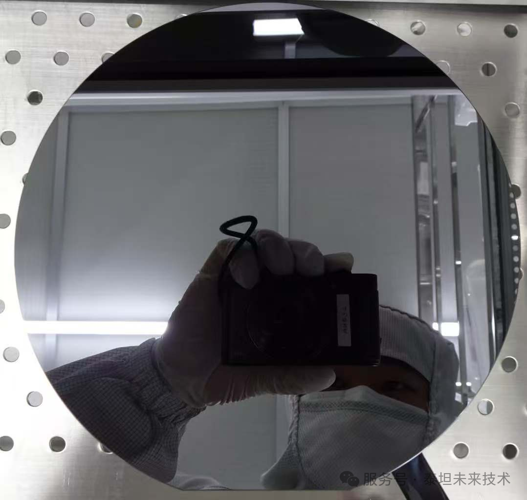
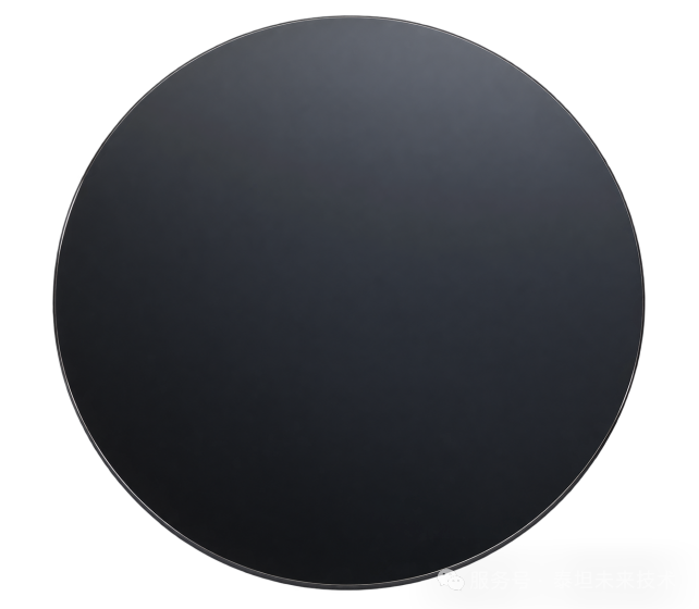
News from the IT Home on October 29th: Hunan Titan Future Technology Co., Ltd. released a press release this month, announcing the launch of China's first 12-inch polycrystalline silicon carbide substrate, aimed at addressing the heat dissipation bottlenecks of AI chips and advanced packaging.
IT Home Query Public Information: 12-inch polycrystalline silicon carbide (SiC) substrates are large-sized ceramic bases with a diameter of about 300 millimeters, composed of many tiny silicon carbide grains. These substrates are primarily used as high thermal conductivity supports and heat dissipation bases in advanced packaging and high-temperature semiconductor processes, helping high-power devices such as AI chips to dissipate heat quickly.
In a press release, the company pointed out that the current market focus in the semiconductor silicon carbide sector is mostly on single-crystal SiC substrates, while polycrystalline silicon carbide supporting materials represent an untapped blue ocean and an invisible yet essential demand in the industry.
High-end polycrystalline materials have long been subject to foreign control, becoming a key bottleneck that restricts the expansion of domestic production lines. The preparation of large-size, dense materials with high purity and matching thermal properties are core technical challenges that need to be overcome urgently.
According to the introduction, this product was developed through a full-process original research and development by the team over a period of more than two years. During this time, they consumed two vapor deposition furnaces and overcame technical challenges such as material densification, large-size molding, and stress regulation.
In terms of key performance, the deposition rate of this substrate reaches 60 micrometers per hour, which is significantly higher than the 10 to 20 micrometers level of domestic and international competitors; the minimum resistivity can be less than 1 milliohms per centimeter, which is better than the approximately 10 milliohms per centimeter level of foreign competitors; there are fewer than 0.1 hole defects per square centimeter, which helps to improve chip yield.
The product has currently passed TSMC's relevant certification tests and samples have been sent to Samsung. At the same time, cooperation is being pursued with companies such as Google and NVIDIA. The project is in the transition phase from sample verification to small-scale trial production, and it is expected that mass supply will gradually begin after 2027.
In 2026, the company invested in a new project to build an industrial base for high-purity and high-density silicon carbide components and polycrystalline substrates. Once fully operational, it will be capable of producing 200,000 pieces of high-performance silicon carbide and tantalum carbide coated products for semiconductors annually.
According to the official introduction, the newly launched 12-inch Poly-SiC polycrystalline substrate, which is a first in China, has achieved breakthroughs in several key indicators: relying on self-developed core technologies such as vapor deposition and supercritical multiphase TaC coating, the product has achieved a super high thermal conductivity of ≥300W/(m·K), which far exceeds the average level of international advanced semiconductor material manufacturers. At the same time, it features zero long cracks, micro-cracks, and extremely low pore defects, possessing excellent thermal properties and structural stability, thus completely breaking the foreign technological monopoly in large-size formation and high-purity preparation.
The product is aimed at two core use cases:
- AI Chip Advanced Packaging Heat Dissipation Substrate: Relying on the excellent thermal conductivity of Poly-SiC (2-3 times that of traditional AIN / Cu solutions), it provides superior adaptability, forming efficient heat conduction channels to solve heat dissipation issues. The company claims that its developed polycrystalline silicon carbide composite substrate saves nearly 20% in cost compared to current industry technologies.
- Composite Substrate and Etching Core Components: Domestic guidelines for single-crystal silicon carbide substrates are restrictive, so large-scale mass production and cost reduction are achieved through composite substrates. The etching ring components have increased the customer's processing yield by 60%.
refer to:
Debut at the 6th Carbon-based New Materials Industry Innovation and Development Conference | The country's first 12-inch Poly-SiC polycrystalline substrate attracts industry attention
Changsha produces China's first 12-inch polycrystalline silicon carbide substrate, solving the heat dissipation problem of high-power chips | Xiangxin Tuqiang