









As advanced manufacturing processes continue to advance towards 1nm and below, traditional GAA nanoscale transistor technologies face increasingly significant challenges in terms of leakage current, mobility, parasitic resistance, and variations in manufacturing processes.
On September 29th local time, GlobalWafers Group ( Lam Research ), one of the top three wafer manufacturing equipment manufacturers in the world, proposed a self-alignment complementary metal-oxide-semiconductor field-effect transistor ( SA-CFET ) architecture that is expected to further advance CMOS transistors to 10 Å (1nm) and below.
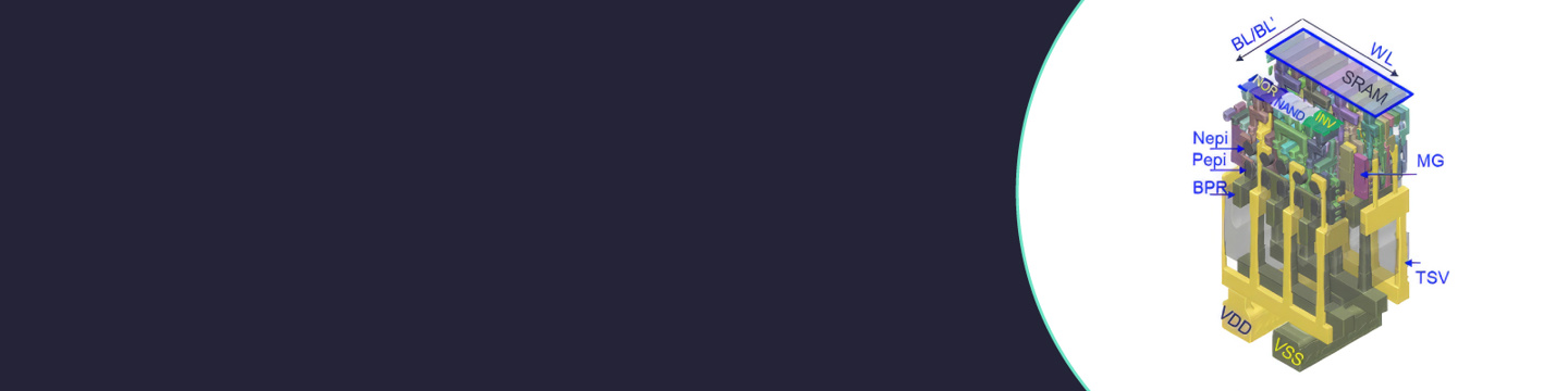
The core of SA-CFET lies in three self-alignment process modules: SA-BPR (self-aligned buried power rails), SA-CT (self-aligned contacts), and SA-TSV (self-aligned silicon vias). This architecture adopts a non-metal gate cutting design and intermediate dielectric isolation (MDI) to achieve separation of work functions, while maintaining compatibility with the N3 specifications (42nm contact gate pitch, 21nm metal pitch). It transforms steps that originally required extremely high overlay alignment precision into self-alignment processes.
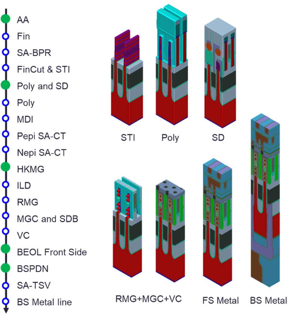
Ferrum Group stated that its Semiverse Solutions team utilized SEMulator3D digital twin technology for modeling, and conducted process flow and device structure verification on the SA-CFET architecture.
The modeling results show that this architecture can be used to construct 6T SRAM units, as well as logical units such as NOT (NOT gate), NAND (NOT gate), and NOR (OR NOT gate). Among them, the area of the 6T SRAM bit (bit) unit is 0.0094 μm², which is a 52.7% reduction compared to N3 and a 19% reduction compared to the A7 CFET design.
IT Note: CFET refers to a complementary metal-oxide-semiconductor field-effect transistor (CMOSFET), which is a transistor architecture that stacks NMOS and PMOS devices vertically. Compared to the traditional method of arranging these two types of transistors side by side, CFET allows for a higher device density within the same planar area, while also increasing the effective channel width and improving the device's electrostatic control capabilities.
Fering Group believes that as transistor sizes continue to shrink, the current advanced silicon-based GAA nanosheet architecture may gradually face limitations due to physical and manufacturing factors. For example, as the gate length is shortened, the source-drain tunneling effect may increase, leading to higher leakage current; further thinning of the channel may result in decreased mobility, surface scattering, and increased manufacturing difficulties. In addition, the reduction in device size also makes contact resistance and parasitic resistance more prominent, and dimensional and positional deviations during the manufacturing process may have a more significant impact on the yield of nodes below 10 Å.
In this case, it becomes increasingly difficult to continue increasing the density of nanosheet transistors merely by reducing the active region, gate, and metal interconnect spacing. CFET attempts to further increase transistor density by vertically stacking NMOS and PMOS, without relying solely on reductions in planar size.
However, CFET itself also faces integration challenges such as complex metal gate isolation and crowded contact areas. As the size continues to decrease, these related issues may further intensify.
To address these issues, Fanlin Group proposes to expand the marginal placement error window using the SA-BPR, SA-CT, and SA-TSV modules, while also alleviating the contact congestion problem in the vertical stacking structure of CFET, thereby enhancing the process margin.
This architecture also adopts a non-metallic gate cutting scheme and achieves function separation through intermediate dielectric isolation ( MDI ). Fanlin Group states that SA-CFET can maintain compatibility with N3, including a 42nm contact gate pitch ( CPP ) and a 21nm metal pitch, and converts some process steps that are sensitive to overlay alignment precision into self-aligning processes to reduce manufacturing difficulties.
In terms of design verification, the digital twin process model shows that SA-CFET is capable of implementing logical standard units such as 6T SRAM as well as NOT, NAND, NOR, etc. Moreover, there is no need for metal gate segmentation within a single fin, which allows for a simplification of the process flow. The complete three-dimensional interconnect network has also been verified through digital twin simulation, indicating that this architecture can support more complex internal wiring of the units.
In terms of process robustness, model verification shows that all key contact layers have a minimum overlay window of 10nm, and no open circuit or short circuit failures were observed in the relevant simulations. Lamina Group believes that this architecture has a considerable process margin. However, it should be noted that the above results come from digital twin process modeling and design verification, and do not imply that SA-CFET has already entered the mass production phase.
The Belgian Microelectronics Research Center ( imec ) released a process roadmap in July of this year, predicting that by 2038 it is possible to achieve 0.3 nanometer ( A3 ) level technology. It also clearly stated that the CFET vertical stacking architecture is the key solution to break through physical limitations and continue Moore's Law.
In the CFET research update released in September, imec further indicated that starting from the A7 logic node, the industry may shift to a transistor architecture based on CFET to support standard cell heights of 4.5 tracks and below.
The SA-CFET solution of Fanlin Group is a modeling study that explores the path for self-alignment process integration in this direction. Its conclusions are based on simulation verification, and actual mass production verification still awaits support from subsequent hardware data.
Fering Group stated that the multi-autocalignment process adopted by SA-CFET can achieve design rules that are comparable to, or even more relaxed than, current or traditional semiconductor manufacturing processes. At the same time, it demonstrates advantages in terms of SRAM area and CFET integration. The company believes that this architecture has the potential to circumvent some of the issues faced during further scaling of nanosheet transistors through larger effective channel widths and better electrostatic control, providing a potential architectural solution for CMOS scaling at 10 Å and below nodes.
Related Reading:
Intel 18A Process Test Results: M0 with a pitch of 36nm, GAA with a pitch of 76nm, Power Via used only for logic chips