












IT News on October 24th: On October 22nd local time, Dwarkesh Patel released an interview video with Intel's Chief Technology Officer, Puskar Ranad ( Pushkar Ranade ).
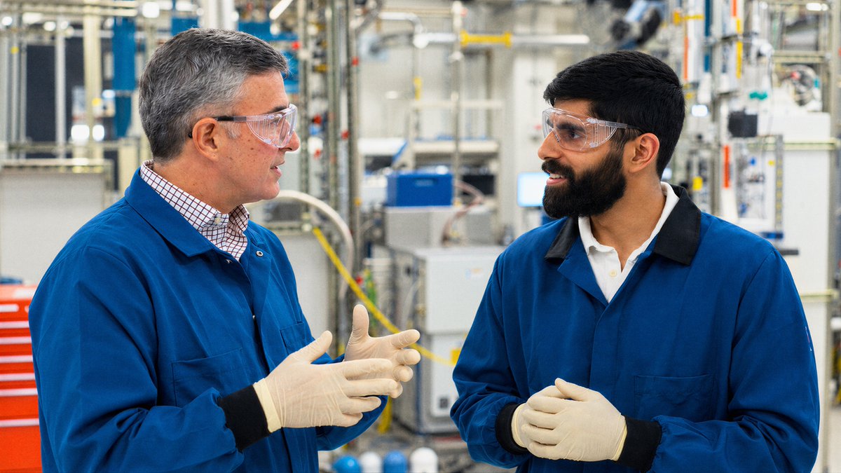
Larnard stated that from a process technology perspective, the gap between Intel and TSMC has narrowed to just a few percentage points, but catching up with TSMC's manufacturing scale will still be a slow process. He emphasized that compared to simply pursuing a slight lead in performance or chip area density, it is more important to advance processes on time, improve yield rates, and rapidly expand production capacity.
He pointed out that TSMC's current wafer manufacturing scale is significantly larger than that of Intel. The competition between the two companies involves not only technical specifications but also the ability to produce a large number of advanced chips stably. He stated that if we only consider technical levels, Intel is already close to TSMC, but there may still be a gap of a few percentage points in indicators such as performance, power consumption, and area density.
He believes that the competition in advanced manufacturing processes cannot be judged solely by the results of individual benchmark tests. When there is a generation gap in process technology, the difference may be quite evident; however, when the technical levels of both parties are close, manufacturing execution capability, yield rates, and the speed at which production capacity can be increased become more important factors.
Lanard pointed out that even if there are a few percentage points of difference in performance or area density, as long as the process can be advanced on time and a high yield can be maintained, there is still a chance to make progress in the competition.
In addition, Lardner also discussed the limitations faced by the expansion of advanced chip production capacity during the interview. He stated that even if Intel wishes to significantly increase the output of advanced process wafers, the global supply capacity of semiconductor manufacturing equipment is unlikely to support a tenfold increase in production; under current conditions, doubling production is more feasible. He pointed out that EUV lithography equipment is one of the main bottlenecks, but there are also shortages in other manufacturing equipment.

In the same interview, Chris Os, Vice President and General Manager of Intel's Manufacturing, Development, and Customer Collaboration Department, discussed high-numeral-aperture extreme ultraviolet lithography (High - NA EUV) technology. He stated that Intel uses a backside power supply architecture, which moves the power supply network to the back of the wafer, reducing the pressure on the wiring spacing on the front side of the wafer. As a result, High - NA EUV equipment can be used directly in some process layers.
IT Note: By increasing the numerical aperture of the optical system from 0.33 in traditional EUV devices to 0.55, NA EUV further enhances lithography resolution. According to device parameters, this technology can achieve a resolution of approximately 8nm, which helps to create finer patterns in a single exposure and reduces the multiple patterning steps required for some process layers.
Oss explained that in traditional chip design, both the power supply lines and signal lines require space on the front side of the wafer. Intel has moved the power supply network to the back side of the wafer through backside power supply technology, freeing up space for the transistors and signal interconnect lines on the front side. This reduces the spacing requirements for certain components, allowing them to be manufactured in a single exposure using High - NA EUV.
Oss believes that Intel and TSMC adopt different technical architectures, therefore they will come to different conclusions regarding the economic benefits of High - NA EUV. It is reported that in some of the process designs discussed, TSMC requires a tighter line pitch and still needs to use a double-exposure process to manufacture the relevant graphics.
Oss also revealed that Intel's 14A process has provided High - NA EUV as an optional option in the process design toolkit (PDK) to customers. Intel will discuss whether to adopt this technology on a case-by-case basis according to the needs of different customers, rather than requiring all customers to use it uniformly. PDK provides the process rules and models required for chip design to external customers, which is an important foundation for them to utilize wafer foundry services.
Larnard also stated that when transitioning from the 18A process to the 14A process, Intel expects to be able to reuse about 80% of the equipment, but some new manufacturing equipment will still be required for the new process. He pointed out that the current delivery cycle for ordered equipment may be around 18 months, and if new wafer factories need to be built as well, the time to start production could be further delayed.
Related Reading:
- Intel claims to double its leading wafer production, while AI's computing power expansion hits a ceiling due to the supply chain.
- Intel's CEO Chen Liwu says that China's chip manufacturing "is not far behind at present"
- Intel's foundry head predicts that the performance of its own 1.4nm process will be within 5% of TSMC's